



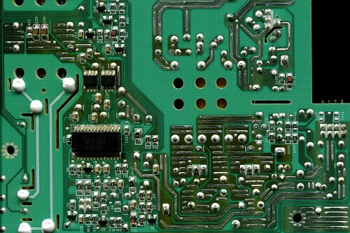
In electronics and datacom manufacturing, data rates keep climbing while hardware keeps getting denser, and those two trends work against each other inside every connector, contact, and housing on a board. Electronics and datacom manufacturing decides whether a design’s thermal and signal targets hold: stamping precision sets contact geometry, plating and material selection set the performance ceiling, insert molding seals the interconnect, and shielding strategy determines what a conductor picks up. A part that models well can still underperform if the process behind it introduces variation the design never accounted for.
Data rates keep climbing and hardware keeps getting denser. Those two trends work against each other inside every connector, contact, and housing on a board. Electronics and datacom manufacturing sits at the point where a design’s thermal and signal targets either hold up or quietly fall apart.
A part that models well can still underperform if the tooling, plating, or molding process behind it introduces variation the design never accounted for. For hardware engineers and sourcing managers, that makes the manufacturing partner decision as consequential as the design decision itself.
The Two Constraints That Dominate Electronics and Datacom Manufacturing
Two physical constraints dominate component design once a product moves past the concept stage. The first is heat. Power density rises as enclosures shrink, and the metal and polymer parts inside have to carry current, dissipate energy, and hold their shape without drifting out of tolerance. The second is signal integrity. As switching speeds increase, small changes in contact geometry, surface finish, or dielectric spacing start to matter in ways they never did at lower frequencies.
Neither constraint is solved on the drawing board alone. Both are decided again, part by part, on the production floor. That is why electronics and datacom manufacturing has become less about buying a component to print and more about matching a design intent to a process that can reproduce it.
Once on the drawing board, and again on the production floor. A design can hold both constraints in simulation and still lose them to die wear, uneven plating deposition, or a knit line that forms near a conductor.
Stamping Precision and Contact Geometry
Contact geometry controls normal force, contact resistance, and how much heat a mated pair generates under load. Stamped features that vary from cavity to cavity or shift as a die wears will produce connectors that behave inconsistently, and inconsistency is difficult to design around.
High-speed presses running high-efficiency progressive dies, paired with digital imaging inspection and control systems, keep those features inside a narrow band across long runs. That capability matters directly for press-fit and compliant contact technology, where insertion force and retention depend on burr control and edge condition. It also matters for impedance-controlled Gigabit transmission line configurations, where the spacing and profile of stamped conductors influence electrical behavior. In electronics and datacom manufacturing, the die is not a supporting detail. It is the mechanism that determines whether a contact performs the same way on the last part as it did on the first.
Each electronics and datacom manufacturing decision maps to a specific thermal or electrical consequence.
| Production Decision | Thermal or Electrical Effect | What Controls It |
|---|---|---|
| Contact geometry | Normal force, contact resistance, heat at the mated pair | Progressive die condition and in-line imaging inspection |
| Plating and base metal | Conductivity, corrosion resistance, wear over mating cycles | Material selection settled before high-volume tooling |
| Resin selection | Heat deflection, dimensional stability, dielectric behavior | Mold design and validated process window |
| Encapsulation quality | Voids, flash, or knit lines near a conductor | Insert molding under the same roof as stamping |
| Shielding strategy | What the conductor picks up from its neighbors | Designed into the part, not added afterward |
Plating and Material Selection in Electronics and Datacom Manufacturing
Base metal and plating choices set the ceiling on both thermal and electrical performance. Conductivity, spring characteristics, corrosion resistance, and wear behavior all trade against one another, and against cost. A finish that survives repeated mating cycles may not offer the lowest contact resistance, and the alloy with the best conductivity may not hold the spring force a latch needs over time.
These are engineering conversations, not purchasing line items. Getting them right early is one reason design services and rapid prototyping belong in the same building as production. When a manufacturer can build a prototype, test it, adjust a material or finish, and carry that change straight into tooling, the feedback loop stays short. Electronics and datacom manufacturing works best when material selection is settled before high-volume tooling is committed, not after.
Insert Molding and Sealed Interconnects
Insert molding is one of the clearest examples of how electronics and datacom manufacturing solves thermal and signal problems at the process level. It places stamped metal into a molded polymer body in a single controlled operation. For interconnect solutions, that means fewer assembly steps, tighter positional control of conductors, and a housing that can seal against moisture and contamination. Sealed interconnects matter anywhere hardware lives outside a clean equipment room, including outdoor radios, cabinets, and distributed nodes.
The polymer side carries thermal responsibility too. Resin selection affects heat deflection, dimensional stability, and dielectric behavior, and the mold design affects how uniformly the material fills around metal inserts. Voids, flash, or knit lines near a conductor can change electrical performance and create long term reliability risk. Having tool design, tool fabrication, stamping, and molding under one roof keeps those decisions coordinated rather than negotiated across suppliers.
Shielding, RFI and EMI Control, and High-Speed Data
Signal integrity is partly about what a conductor carries and partly about what it picks up. Shielding strategy, grounding paths, and the physical relationship between conductors and return paths all shape how a component behaves in a dense assembly. Embedded signal integrity and RFI or EMI solutions are most effective when they are designed into the part rather than added afterward as a fix.
Expertise in electronic component and flex circuit integration supports this work, as does experience with hybrid packaging that combines optical, wire, and power components, including Power over Ethernet. High-speed data hardware rarely uses one signal type in isolation, and the packaging has to accommodate all of it without letting one path compromise another.
Dimensional Consistency in Electronics and Datacom Manufacturing at Volume
A prototype proves a concept. Volume production proves a process. The gap between the two is where many thermal and signal problems appear, usually as intermittent failures that are expensive to trace back to a root cause.
Consistency at volume comes from disciplined process design, capable tooling, in-process inspection, and automated assembly that removes variation introduced by manual handling. Quality systems support that discipline. NCT holds ISO 9001:2015 and ISO 13485:2016 certification and maintains ISO 14644-1 cleanroom capability, and the company is C-TPAT compliant. For sourcing managers, those systems are a signal that the process is documented and repeatable, which is what protects a design once quantities scale.
Metal stamping, injection molding, insert molding, tool design and fabrication, and automated assembly on one 20 acre campus, so thermal and electrical intent is held from first article through full production.
Single Source Electronics and Datacom Manufacturing at NCT
New Concept Technology operates a 200,000 square foot facility on a 20 acre campus in Emigsville, Pennsylvania, with nearly 30 years of manufacturing experience behind it. The company serves automotive, medical, industrial, telecommunications, electronics and datacom, and aerospace and defense customers, and works with Fortune 500 companies as a single source, design through manufacturing partner. The NCT Mexico division, NECONTECH, supports nearshoring for programs that need production closer to North American demand.
That combination is what makes integrated contract manufacturing valuable to datacom OEMs. In-house process design, tooling fabrication, and high-volume manufacturing expertise help maximize quality while minimizing cost, and expertise in interconnect solutions supports standard and hybrid packaging across optical, wire, and power components. Electronics and datacom manufacturing rewards partners who can hold thermal and electrical intent from first article through full production.
Frequently Asked Questions
What are the two dominant constraints in electronics and datacom component design?
Heat and signal integrity govern electronics and datacom manufacturing. Power density rises as enclosures shrink, so metal and polymer parts must carry current, dissipate energy, and hold shape. As switching speeds increase, small changes in contact geometry, surface finish, or dielectric spacing start to matter in ways they did not at lower frequencies.
Why does stamping precision affect electrical performance?
In electronics and datacom manufacturing, contact geometry controls normal force, contact resistance, and how much heat a mated pair generates under load. It also drives impedance in high-speed transmission line configurations, because impedance is a function of conductor dimensions and their relationship to surrounding dielectric.
How do plating and base metal choices trade against each other?
Conductivity, spring characteristics, corrosion resistance, and wear behavior all trade against one another and against cost. A finish that survives repeated mating cycles may not offer the lowest contact resistance, and the alloy with the best conductivity may not hold the spring force a latch needs over time.
What does insert molding contribute to interconnect reliability?
It places stamped metal into a molded polymer body in a single controlled operation, which means fewer assembly steps, tighter positional control of conductors, and a housing that can seal against moisture and contamination for hardware installed outside a clean equipment room.
Why should shielding be designed in rather than added later?
Shielding strategy, grounding paths, and the physical relationship between conductors and return paths all shape how a component behaves in a dense assembly. Embedded signal integrity and RFI or EMI solutions are most effective when they are part of the design rather than a fix applied afterward.
What makes the difference between prototype performance and volume performance?
Disciplined electronics and datacom manufacturing: process design, capable tooling, in-process inspection, and automated assembly that removes the variation manual handling introduces. The gap between a working prototype and stable volume is where most intermittent thermal and signal failures appear.
Hold thermal and signal intent from first article to full production.
New Concept Technology combines in-house tooling, high-speed stamping, injection molding, insert molding, and automated assembly with in-process inspection. Contact us to discuss how electronics and datacom manufacturing decisions affect a new program.
Contact Us →Sources
| Organization | Resource |
|---|---|
| IPC (Global Electronics Association) | IPC Standards for Electronics Assembly |
| Encyclopaedia Britannica | Press (Machine Tool): Blanking, Forming, and Coining |